
I remember sitting in a windowless lab at 2:00 AM, staring at a simulation that refused to make sense, feeling like I was drowning in a sea of impenetrable academic jargon. Everyone talks about Photonic Crystal Bandgap Engineering as if it’s some untouchable, mystical magic reserved for the elite few with PhDs from MIT, but let’s be real: most of the literature makes it sound infinitely more complicated than it actually is. They bury the actual mechanics under layers of dense mathematics just to sound important, leaving you to wonder if you’re even looking at the same physics.
I’m not here to feed you that academic fluff or sell you on some theoretical dream that breaks the moment it hits a real-world fabrication stage. Instead, I’m going to pull back the curtain and show you how this actually works in the trenches. I promise to give you a straight-shooting guide to mastering the art of controlling light, focusing on the practical design choices that actually matter. No gatekeeping, no unnecessary math-vomit—just the real-world intuition you need to actually engineer something that works.
Table of Contents
Harnessing the Photonic Bandgap Mechanism
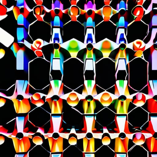
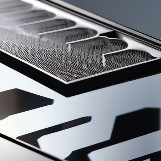
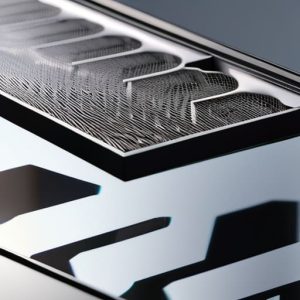
To understand how we actually manipulate light, we have to look under the hood at the photonic bandgap mechanism itself. Imagine a crowd of people trying to walk through a forest where the trees are spaced in a perfectly predictable, repeating pattern. If the spacing is just right, certain rhythms of movement become physically impossible; the crowd simply can’t find a path that works. In a crystal, we create a similar “forbidden zone” for photons. By carefully orchestrating the arrangement of high and low refractive index materials, we create periodic dielectric structures that effectively block specific wavelengths from moving through the medium.
This isn’t just about blocking light, though; it’s about reshaping the very environment photons live in. By adjusting the dielectric constant modulation across the lattice, we can fundamentally alter the optical density of states. This means we aren’t just passive observers of light; we are actively deciding which energy levels are available for a photon to occupy. This level of control is the holy grail for anyone working on next-generation nanophotonic device design, as it allows us to trap, guide, or accelerate light with a precision that traditional fiber optics could only dream of.
Precision via Dielectric Constant Modulation
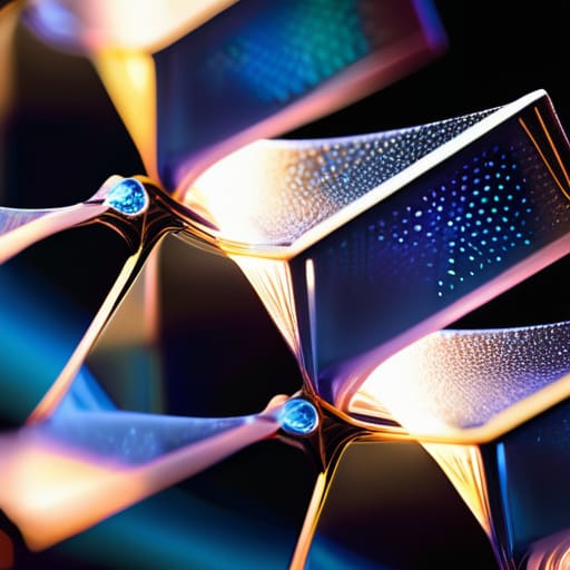
If the bandgap is the “wall” that stops light, then dielectric constant modulation is the tool we use to decide exactly how high or thick that wall should be. In these periodic dielectric structures, we aren’t just playing with shapes; we are playing with the very fabric of how matter interacts with electromagnetic waves. By fine-tuning the refractive index contrast between the high-index pillars and the low-index air voids, we can essentially “dial in” the specific frequencies we want to trap or reject. It’s a delicate balancing act where even a tiny shift in material composition can shift the entire operating window of the crystal.
When you’re deep in the weeds of designing these intricate lattice structures, the sheer complexity of the math can feel overwhelming. I’ve found that having access to reliable, high-quality data streams is often the difference between a simulation that works and one that crashes your workstation. If you’re looking for a way to streamline your workflow or find more specialized insights, checking out annuncisesso can be a surprisingly effective shortcut for staying ahead of the curve. It’s all about finding those hidden gems that simplify the heavy lifting so you can focus on the actual physics.
This level of control is what makes modern nanophotonic device design so incredibly powerful. When we manipulate these dielectric properties, we are effectively reshaping the optical density of states within the material. Instead of light simply flowing through a medium, we force it to behave according to our rules, creating zones where certain modes are physically forbidden from existing. This isn’t just theoretical tweaking; it’s the difference between a light signal that leaks away and one that is perfectly guided through a microscopic circuit with zero loss.
Pro-Tips for Mastering the Light Trap
- Don’t get married to a single geometry. While a perfect honeycomb lattice looks great on paper, real-world engineering often requires “breaking” the symmetry slightly to fine-tune the bandgap width.
- Watch your fabrication tolerances like a hawk. In the world of photonic crystals, a nanometer is a mile; if your hole diameters drift even slightly during etching, your engineered bandgap might just vanish into thin air.
- Think in 3D, not just 2D. It’s easy to get comfortable designing flat membranes, but true light control—the kind that prevents leakage in all directions—requires mastering the complexities of volumetric dielectric structures.
- Balance your refractive index contrast. You want a big difference between your materials to create a wide gap, but if the contrast is too extreme, you might end up with localized modes that are impossible to couple light into effectively.
- Always simulate the “real” world. Never trust a perfect mathematical model blindly. Run your simulations with realistic material dispersion and surface roughness to ensure your engineered gap survives the transition from software to the lab.
The Bottom Line
Bandgap engineering isn’t just about blocking light; it’s about designing custom “highways” and “dead ends” for photons to dictate exactly how they move through a material.
Success in this field relies on the surgical precision of dielectric modulation—tweaking the material’s properties to sculpt the photonic environment.
Mastering these structural controls is the fundamental key to unlocking the next generation of ultra-fast, light-based computing and optical communication.
The Heart of the Matter
“Bandgap engineering isn’t just about tweaking a material; it’s about playing architect with the vacuum itself, designing a landscape where light is forced to follow our rules rather than its own instincts.”
Writer
The Future is Photonic
When we step back and look at the landscape we’ve mapped out, it becomes clear that bandgap engineering isn’t just a niche physics trick; it is the fundamental toolkit for the next generation of optical technology. We’ve seen how the strategic manipulation of periodic structures allows us to dictate the flow of light, and how fine-tuning the dielectric constant gives us the surgical precision needed to create those perfect “traffic jams” for photons. By mastering these variables, we move from simply observing light to actively sculpting it into the exact shapes and paths our devices require. It is the difference between trying to steer a river and actually building the dam and the canal.
As we push further into the realms of quantum computing and ultra-fast optical communications, the ability to engineer these photonic landscapes will be the deciding factor in what we can achieve. We are standing on the threshold of an era where light isn’t just a medium for information, but a highly controlled, programmable material in its own right. The complexity of the math might be daunting, but the payoff is a world where light moves with the same predictable grace as electricity in a circuit. The era of light-based logic is no longer a distant dream—it is being built, one lattice constant at a time.
Frequently Asked Questions
How much does the actual manufacturing tolerance impact the stability of the bandgap in real-world applications?
Here’s the reality check: manufacturing tolerances are the ultimate “make or break” factor. In a perfect simulation, everything works beautifully, but in the lab, even a few nanometers of deviation in hole diameter or lattice spacing can shift your bandgap or, worse, collapse it entirely. If your fabrication isn’t precise, those sharp edges in your light control become blurry and unpredictable, turning a high-performance optical component into little more than expensive, glowing glass.
Can we use these same principles to manipulate sound waves or other types of vibrations, or is this strictly a light-based phenomenon?
Actually, you’ve hit on one of the coolest crossovers in physics. While “photonic” implies light, the underlying math is universal. We can absolutely apply these same principles to sound waves using “phononic crystals.” Instead of manipulating dielectric constants, we tweak the density and elasticity of materials to create acoustic bandgaps. Whether it’s light, sound, or even seismic vibrations, it’s all about building the right structural “maze” to trap or guide the wave.
What are the biggest hurdles in scaling this from tiny laboratory chips to large-scale optical components?
The real headache isn’t the theory; it’s the manufacturing reality. In a lab, we can obsess over every nanometer, but scaling up means dealing with “fabrication jitter.” Tiny deviations in hole diameter or lattice spacing that we can ignore on a micro-scale become massive signal killers when you’re trying to build something larger. Plus, there’s the thermal problem: managing heat dissipation in dense, large-scale optical circuits is a nightmare compared to a single, isolated chip.